SCOPE Solution
CLOCKED LATCH
SCOPE ACT 4
Prerequisites
Unlocks
sc_a4_11_clocked_latch locked
Par power800
Par lines18
Par chips3
Objective
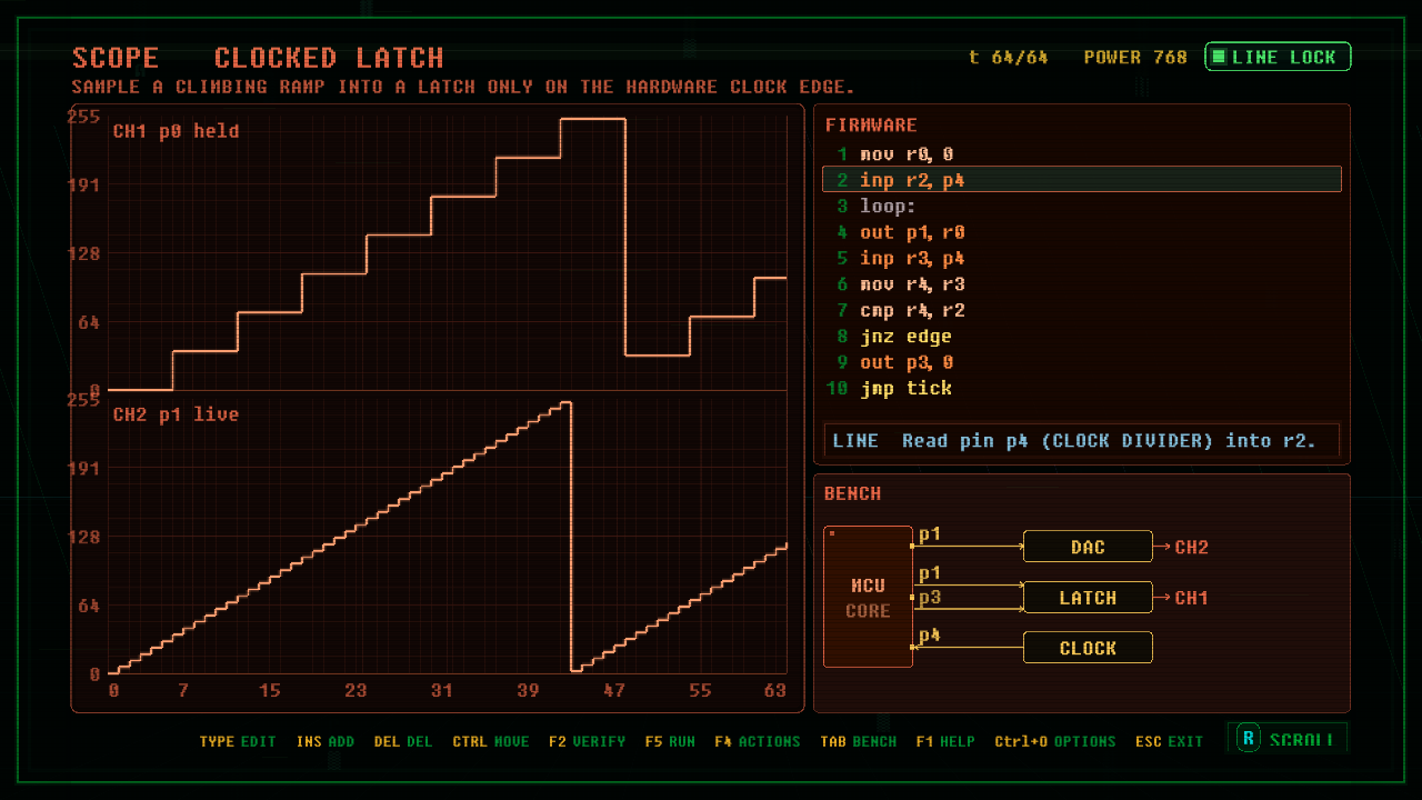
Sample a climbing ramp into a latch only on the hardware clock edge.
Board Data
- Window: 64
- Pins: p1 OUT, p3 OUT, p4 IN, p0 IN
- Channels: p0 ANALOG label=CH1_p0_held, p1 ANALOG label=CH2_p1_live
- Peripherals: DAC data=p1 label=DAC_live_p1, CLOCK in=p4 k=6 label=CLOCK_on_p4, LATCH data=p1 strobe=p3 q=p0 label=LATCH_Q_on_p0
Firmware Solution
; CLOCKED LATCH reference. The CLOCK DIVIDER on p4 toggles every K ticks; the LATCH
; captures the live ramp staged on D (p1) when the strobe (p3) is pulsed and holds it
; on Q (p0). The firmware climbs the live ramp every tick and watches the clock with
; inp; when the clock level changes from the last tick it raises the strobe for that
; one tick, so the latch grabs the current ramp on the hardware edge. The step width
; is the clock period, decided by the hardware, so one firmware tracks every K.
        mov  r0, 0         ; r0 = the live ramp level
        inp  r2, p4        ; r2 = last clock level seen
loop:
        out  p1, r0        ; stage the live ramp on CH2 and the latch D
        inp  r3, p4        ; read the clock level this tick
        mov  r4, r3
        cmp  r4, r2        ; did the clock edge arrive since last tick?
        jne  edge
        out  p3, 0         ; no edge: hold the strobe low
        jmp  tick
edge:
        out  p3, 255       ; edge: pulse the strobe high to capture D into Q
tick:
        mov  r2, r3        ; remember this clock level for the next compare
        slp  1
        add  r0, 6         ; climb the live ramp one step per tick
        jmp  loop
Board Definition
# CLOCKED LATCH. ACT 4. SCOPE waveform board.
# TITLE CLOCKED LATCH
# OBJECTIVE Sample a climbing ramp into a latch only on the hardware clock edge.
# Two chips cooperate: a CLOCK DIVIDER toggles p4 every K ticks, and a LATCH holds
# whatever is staged on its D pin when its strobe is pulsed. The firmware climbs a
# live ramp on CH2 every tick, watches the clock with inp, and pulses the latch strobe
# the moment the clock edge arrives, so the held Q on CH1 is a sample-and-hold
# staircase whose tread width is the clock period. The battery moves K, so a
# transcript with the steps baked at one width diverges on the next: only detecting
# the clock edge and strobing the latch locks every case.
ID sc_a4_11_clocked_latch
WINDOW 64
DIR p1 OUT
DIR p3 OUT
DIR p4 IN
DIR p0 IN
PERIPH DAC data=p1 label=DAC_live_p1
PERIPH CLOCK in=p4 k=6 label=CLOCK_on_p4
PERIPH LATCH data=p1 strobe=p3 q=p0 label=LATCH_Q_on_p0
CHAN p0 ANALOG label=CH1_p0_held
CHAN p1 ANALOG label=CH2_p1_live
CASE k=6
PAR power=800 lines=18 chips=3