SCOPE Solution
BLINK
SCOPE ACT 1
Prerequisites
Unlocks
sc_a1_01_blink locked
Par power15
Par lines6
Par chips1
Objective
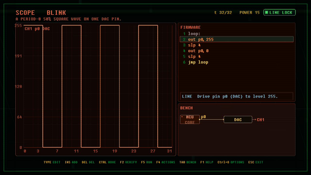
A period-8 50% square wave on one DAC pin.
Board Data
- Window: 32
- Pins: p0 OUT
- Channels: p0 ANALOG label=CH1_p0_DAC
- Peripherals: DAC data=p0 label=DAC_on_p0
Firmware Solution
; BLINK reference: period-8 50% square on p0 (high 4 ticks, low 4 ticks).
; The out before each slp colors that tick and the next n-1 ticks (n total).
loop:
      out  p0, 255      ; latch HIGH
      slp  4            ; ticks T..T+3 sample 255
      out  p0, 0        ; latch LOW
      slp  4            ; ticks T+4..T+7 sample 0
      jmp  loop
Board Definition
# BLINK. ACT 1, analog. The simplest SCOPE board: only slp moves time, so two slp
# counts shape the wave. The MCU drives p0 (an output pin) into the DAC; CH1 watches
# that pin as an analog level 0..255. The reference firmware is sc_a1_01_blink.asm.
# TITLE BLINK
# OBJECTIVE A period-8 50% square wave on one DAC pin.
ID sc_a1_01_blink
WINDOW 32
DIR p0 OUT
PERIPH DAC data=p0 label=DAC_on_p0
CHAN p0 ANALOG label=CH1_p0_DAC
PAR power=15 lines=6 chips=1