SCOPE Solution
CLOCK GATE
SCOPE ACT 2
Prerequisites
Unlocks
sc_a2_11_clock_gate locked
Par power40
Par lines7
Par chips1
Objective
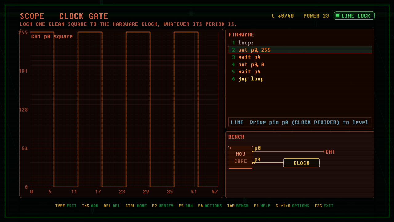
Lock one clean square to the hardware clock, whatever its period is.
Board Data
- Window: 48
- Pins: p0 OUT, p4 IN
- Channels: p0 ANALOG label=CH1_p0_square
- Peripherals: CLOCK in=p4 k=6 label=CLOCK_on_p4
Firmware Solution
; CLOCK GATE reference. The CLOCK DIVIDER on p4 toggles every K ticks. The firmware
; never counts ticks: it drives the square HIGH, WAITs for the next clock edge, drives
; it LOW, and waits again. One full square period is two clock halves, so the output
; stays locked to the hardware for any K in the battery.
loop:
        out  p0, 255       ; square HIGH for this clock half
        wait p4            ; release on the next clock edge
        out  p0, 0         ; square LOW for the next half
        wait p4            ; release on the following edge
        jmp  loop
Board Definition
# CLOCK GATE. ACT 2. SCOPE waveform board.
# TITLE CLOCK GATE
# OBJECTIVE Lock one clean square to the hardware clock, whatever its period is.
# A CLOCK DIVIDER toggles p4 every K ticks. The firmware must never count ticks: it
# WAITs on the clock edge, drives the square HIGH for one clock half, waits again,
# then drives it LOW. The battery moves K, so a counted-slp square tuned to one
# period diverges on the next; only riding the hardware edge locks every case.
ID sc_a2_11_clock_gate
WINDOW 48
DIR p0 OUT
DIR p4 IN
PERIPH CLOCK in=p4 k=6 label=CLOCK_on_p4
CHAN p0 ANALOG label=CH1_p0_square
CASE k=6
PAR power=40 lines=7 chips=1